QCM#
Description#
The Qubit Control Module (QCM) is an instrument dedicated to qubit control using parametrized pulses. These pulses are stored as waveform envelopes in memory and can be adjusted by changing the gain, offset, and phase. This functionality is managed by six on-board Qblox Q1 sequencer processors, which enable the multiplexing of signals.
The QCM occupies a single slot in either the cluster or the DC cluster. It features four SMA female connectors for pulse output and four SMP male pins for triggering external instruments. The module’s operational status is continuously indicated by 6 LED lights.The front of a QCM module is presented below:
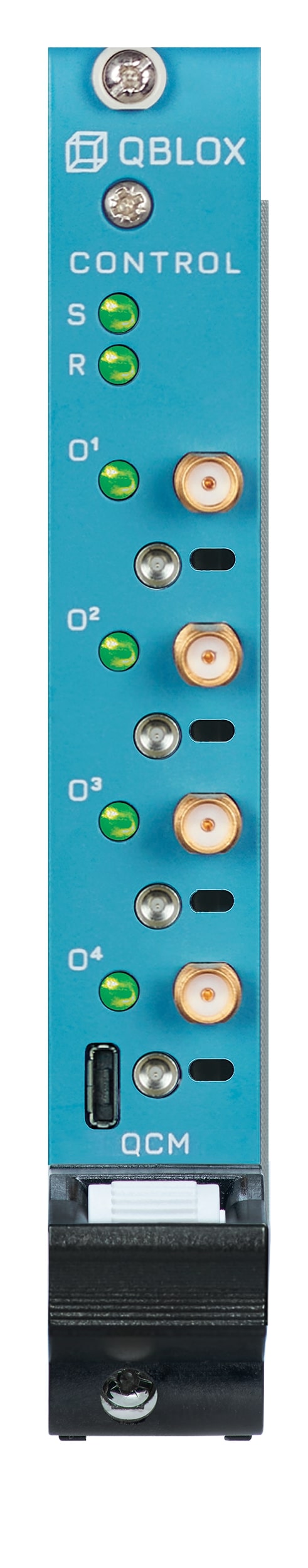
On the front of a QCM module, you will find the following components:
4 x SMA female (receptacle) connectors: 4 outputs (O[1–4] @ 50 Ω).
4 x SMP male (pin) connectors: Marker output channels (0–3.3 V TTL).
6 x status LEDs: See section on Frontpanel LEDs for details.
Pulses are stored as waveform envelopes in memory and can be parametrized by changing gain and offset, and additionally, phase if also modulated. This is all managed by Qblox’s Q1 sequencer processors. The QCM has 6 control sequencers on board, with the following architecture:

Parametrization of pulses is controlled by the AWG of the sequencers, which each have two waveform paths (referred to as path 0 and 1). Using parametrization, the output of these paths can be either independent signals or modulated IQ signals. The two paths of each sequencer can, in turn, be connected to any output pair of the instrument (i.e., O1/2 or O3/4) to control one or more qubits per output. Additionally, each sequencer can control the four marker output channels.
For a list of available features, please go to Features.
Block Diagram#

Features#
1. 10MHz Reference#
Alongside all available modules, the QCM baseband module operates with respect to a 10 MHz reference provided by the cluster.
2. Trigger#
The trigger of the QCM is connected to the cluster and allows for fast synchronization between modules.
3. SYNQ#
The Qblox SYNQ technology enables simple and quick synchronization over multiple instruments, allowing for modules to be started synchronously \( \ll 1\) ns. See section synchronization for more information.
4. LINQ#
The Qblox LINQ technology allows for the results of measurements to be shared between devices, distributing outcomes in < 400 ns.
5. Q1 Sequencers#
The Q1 sequencers are the heart(s) of the QCM instrument. They orchestrate the experiment using a custom low-latency sequence processor specifically designed for quantum experiments. Each QCM has 6 control sequencers to target multiple frequencies with one output.
Each control sequencer has a dedicated AWG path, which enables parametrized pulse generation and readout.
6. Marker Output Channels#
Each sequencer has control over the four marker output channels, with the control of each sequencer being OR’ed to
create the final marker outputs. The markers can be dynamically controlled with the set_mrk instruction of the
sequence processor (see section on latched instructions),
but can also be overwritten with the static marker overwrite parameters ControlSequencer.marker_ovr_en() and
ControlSequencer.marker_ovr_value(). The marker output range is 0–3.3 V TTL. In RF modules, set_mrk is also
used to toggle the switches before the outputs/inputs to enable the respective output/input.
6.1 Setting Markers as Active HIGH/LOW#
The default state of a marker is active high (OFF = 0 V, ON = 3.3 V). Users have the ability to change the marker
output from active HIGH to active LOW (OFF = 3.3 V, ON = 0 V). It can be done using the parameter
QCM.marker0_inv_en(). This inversion of marker default states is possible for all marker channels.
7. Sequencer Multiplexer#
Each of the 6 control sequencers in a QCM has two output streams (path 0 and path 1 also called I and Q). Each of these can be connected to any of the two output DACs using the channel map.
ControlSequencer.connect_out0()connects a sequencer path to an output. For example, to connect the Q path of sequencer 2 to output 1, useqrm.sequencer2.connect_out1("Q"). The argument may be “I”, “Q” or “off”. All the output streams that are connected to the channel map are added together. This may result in clipping.
For more details about multiplexing and its operation on our cluster, please refer to the multiplexed sequencing tutorial.
Note
The default state is that the I quadrature is connected to all even outputs of all sequencers, and Q to odd outputs. This is so that the modules can always play a sequence in their default state.
The channel map may be cleared by setting all connect_out* parameters for all sequencers to ‘off’. The
QCM.disconnect_outputs() convenience function may be used instead.
The QCM supports both an IQ (both paths are modulated for use with an IQ mixer) and a real sequencer mode (only path 0 is modulated, and both paths will be combined at the output). See the user guide page for more details.
8. Digital Offset#
Each output has a dedicated offset step statically configured using the QRM.out0_offset(), QRM.out1_offset()
parameters corresponding to each output channel. This is a digital offset applied on top of the combined signal from all
sequencer paths mapped to the corresponding output channel.
Note
This offset is applied to the signals before the real-time predistortions are applied.
9. Real Time Predistortions#
Each QCM output has real-time predistortion filters that can be used to correct for distortions in the components leading to the device under test (see the page on predistortions).
10. DAC#
The dynamic output range of the QCM’s DACs is 5 Vpp and 50 Ω terminated at 1 GBps.
11. Offset DAC#
The offset DAC allows users to apply a DC offset to the output signal without the risk of clipping the signal at the DAC.
Absolute Maximum Ratings#
Warning
This section shows the absolute maximum ratings of the cluster QCM module. Operation beyond these values can damage the module and cluster!
Parameter |
Condition |
Min |
Typ |
Max |
|---|---|---|---|---|
Voltage applied to output |
-5V |
+5V |
||
Marker load impedance |
66Ω |
Specifications#
Outputs#
Parameter |
Condition |
Min |
Typ |
Max |
|---|---|---|---|---|
Number of channels |
4 |
|||
Output coupling |
DC |
|||
Resolution |
16bits |
|||
Output impedance |
50Ω |
|||
Output range |
In 50Ω load |
+-2.5V |
||
Analog offset voltage range |
+-80mV |
|||
Power Consumption |
38.5W |
Marker Outputs#
Parameter |
Condition |
Min |
Typ |
Max |
|---|---|---|---|---|
Number of markers |
4 |
|||
High voltage |
in high Z load |
3.3V |
||
Low voltage |
0.0V |
Typical Performance#
Output#
Parameter |
Value |
Test specifics |
|---|---|---|
Voltage range |
+-2.5 V |
Measured with a 1MHz block wave in 50Ω load |
Rise time |
<1.4 ns |
Measured with a 1V step in 50Ω load, 10% - 90% |
Settling time |
<8 ns |
Measured with a 1V step in 50Ω load, settled to +-1% |
Overshoot |
<1% |
Measured with a 1V step in 50Ω load |
Crosstalk step |
<-65 dB |
Measured with a 5V step in 50Ω load at 100 MHz |
Crosstalk sine |
<-70 dB |
Measured with a 5Vpp sine wave in 50Ω load at 100 MHz |
Output bandwidth |
>190 MHz |
-3dB point |
>400 MHz |
-9dB point |
|
Output RMS noise |
<100 uVrms |
Based on the bandwidth of 220 MHz at -3dB point |
Wideband noise |
<6.5 nV/sqrtHz |
Noise measured at 121Mhz with 1kHz band and 0V output |
Signal to noise ratio |
>80 dB |
Based on the output RMS noise voltage |
Total harmonic distortion (HD) |
<0.006 |
Measured at 100MHz sine wave up to the fifth harmonic, over the full output voltage swing |
HD2 |
<-45 dBc |
Measured at 100MHz sine wave up to the fifth harmonic, over the full output voltage swing |
HD3 |
<-50 dBc |
Measured at 100MHz sine wave up to the fifth harmonic, over the full output voltage swing |
Total harmonic distortion (HD) |
<0.0015 |
Measured at 100MHz sine wave up to the fifth harmonic, at 1Vpp output voltage |
HD2 |
<-65 dBc |
Measured at 100MHz sine wave up to the fifth harmonic, at 1Vpp output voltage |
HD3 |
<-60 dBc |
Measured at 100MHz sine wave up to the fifth harmonic, at 1Vpp output voltage |
Product Compliance Information#
Compliance with EMC requirements is only guaranteed with cables up to 30 meters.