QRM-RF#
Description#
The Qubit Readout Module (QRM-RF) provides all the necessary capabilities for qubit readout, eliminating the need to manually up and down-convert signals. This allows the device to synthesize and acquire signals in the 2-18.5 GHz range using internal RF conversion stages. Each module is equipped with two SMA female connectors—one for signal output and one for signal input—and two SMP male connectors for marker outputs. The operational status of the QRM-RF is continuously monitored by four LED lights. The front of a QCM module is presented below:
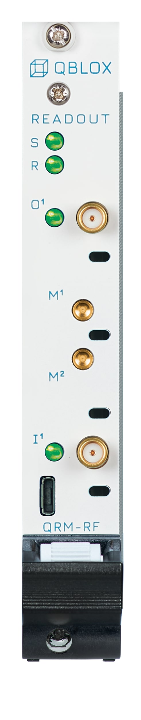
On the front of a QRM-RF module you will find the following components:
2 x SMA female (receptacle) connectors: 1 output (O[1]: @ 50 Ω) ; and 1 input channel (I[1]: @ 50 Ω).
2 x SMP male (pin) connectors: Marker output channels (0-3.3 V TTL).
4 x status LEDs: See section Frontpanel LEDs.
The operation of the module is similar to the standard QRM, with 6 readout sequencers onboard. Each sequencer is connected to the output markers, as well as the input and output paths. Using parametrization, each sequencer can target one qubit for readout, allowing multiplexed readout of multiple qubits on the same channel. The AWG paths can generate the readout pulses and the acquisition paths can process the returned readout data. The acquisition path supports any combination of three acquisition modes:
Scope: Returns the raw input data.
Integration: Returns the result after integrating the input data; optionally based on an integration function stored in memory.
Thresholded: Returns the binary qubit value after thresholding the integrated value.
The results of the acquisitions are returned to the user through the qblox_instruments driver.
For a list of available features please go to Features
Block Diagram#

The QRM-RF module contains the following features:
Features#
1. 10MHz Reference#
Alongside all modules available, the QRM-RF module operates with respect to a 10MHz reference provided by the cluster.
2. Trigger#
The trigger of the QRM-RF is connected to the cluster and allows for fast synchronization between modules.
3. SYNQ#
The Qblox SYNQ technology enables simple and quick synchronization over multiple instruments, allowing for modules to be started synchronously \( \ll 1\) ns. See section synchronization for more information.
4. LINQ#
The Qblox LINQ technology allows for the results of measurements to be shared between devices, distributing outcomes in < 400 ns.
5. Q1 Sequencer#
The Q1 sequencers are the heart(s) of the QRM instrument. They orchestrate the experiment using a custom low-latency sequence processor specifically designed for quantum experiments. Each QRM has 6 readout sequencers to target multiple qubits with one instrument.
Each readout sequencer has a dedicated AWG path and an acquisition path, which enables parametrized pulse generation and readout.
6. Marker output channels#
Each sequencer has control over the four marker output channels, with the control of each sequencer being OR’ed to
create the final marker outputs. The markers can be dynamically controlled with the set_mrk instruction of the
sequence processor (see section on latched instructions),
but can also be overwritten with the static marker overwrite parameters ReadoutSequencer.marker_ovr_en() and
ReadoutSequencer.marker_ovr_value(). The marker output range is 0-3.3 V TTL. In the QRM-RF module set_mrk is
also used to toggle the switches before the outputs/inputs to enable the respective output/input. For the QRM-RF module,
bit indices 0 & 1 correspond to input 1 and output 1 switches respectively, indices 2 & 3 correspond to marker outputs 1
and 2 respectively.
6.1 Setting Markers as Active HIGH/LOW#
The default state of marker is active high (OFF = 0V, ON = 3.3V). Users have the ability to change the marker output
from active HIGH to active LOW ( OFF = 3.3 V, ON = 0V). It can be done using the parameter
QRM_RF.marker0_inv_en(). This inversion of marker default states is possible for all marker channels. Here
marker0 and marker1 correspond to bit indices 2 & 3 respectively in in the argument of set_mrk as mentioned above.
7. Sequencer Multiplexer#
Each of the 6 readout sequencers in a QRM-RF has one complex output stream. This can either be connected to or disconnected from the output using the channel map. Similarly, the input may be be connected to or disconnected from the input stream of any sequencer.
ReadoutSequencer.connect_out0()connects a sequencer output stream to an output. For example, to connect the IQ path of sequencer 2 to output 1, useqrm.sequencer2.connect_out1("IQ"). The argument may be “IQ” (True) or “off” (False). All the output streams that are connected to the channel map are added together. This may result in clipping.ReadoutSequencer.connect_acq()connects an input to a sequencer path. For example, to connect input 1 to the IQ path of sequencer 2, useqrm.sequencer2.connect_acq("in1"). The argument may be “in0”, “in1” or “off”. All the sequencers whose input streams are connected to an input receive the same input samples.
For more details about multiplexing and its operation on our cluster, please refer to the multiplexed sequencing tutorial.
Note
The default state is that the input and output stream of all sequencers is connected to input0 and output0. This is so that the modules can always play a sequence in their default state.
The channel map may be cleared by setting all connect_out* and connect_acq_* parameters for all sequencers to ‘off’.
The QRM_RF.disconnect_outputs() and QRM_RF.disconnect_inputs() convenience functions may be used
instead.
8. Digital Offset#
Each sequencer has a dedicated offset step for both path 0 and 1, which can be statically configured using the
ReadoutSequencer.offset_awg_path0() parameters. However, the offset can also be dynamically controlled using the
set_awg_offs instruction of the sequence processor which enables pulse parametrization. (see section on
latched instructions). The static and dynamic offset
controls are complementary.
Note
This offset is applied to the signals before the mixer and cannot be used for DC offset correction if the mixer is enabled.
9. DAC and ADC#
The dynamic output range of the QRM-RF’s DACs is 5 Vpp and 50 Ω terminated at 1GBps.The maximum input range of the QRM’s ADCs is 2 Vpp and 50 Ω terminated.
Note
The 12-bit ADCs have a fixed range of 2 Vpp. When performing acquisitions the input should be an order of magnitude such that the resolution (0.5mV) of the ADC can accurately define the measured signal. Gain or attenuation stages may be required at the input to compensate for this. See 13. Variable Attenuator for the attenuation onboard the device.
10. Offset DAC#
The offset DAC allows users to apply a DC offset to the output signal without the risk of clipping the signal at the DAC.
11. Local Oscillator#
The QRM-RF module comes equipped with its own built-in local oscillator capable of generating signals between 2.5 and 18GHz for IQ mixing.
12. IQ Mixer#
The QRM-RF module also has onboard IQ mixers for both the output and acquisition. The LO’s of these internal mixing stages are capable of sweeping between 2-18.5GHz. This allows for the generation and acquisition of signals at the qubit and readout resonator frequency respectively.
13. Variable Attenuator#
The QRM-RF module has a variable attenuator, which can be programmed, on both the input and output terminals. The output attenuation can be programmed to be between 0 to 60 dB in 2 dB steps whilst the input attenuation can be set between 0 to 30 dB in 2 dB steps.
14. Output Switch#
The output terminal of the QRM-RF can be toggled with an inbuilt switch.
Absolute Maximum Ratings#
Warning
This section shows the absolute maximum ratings of the cluster QRM-RF module. Operation beyond these values can damage the module and cluster!
Input#
Parameter |
Condition |
Min |
Typ |
Max |
|---|---|---|---|---|
Input Power |
15 dBm |
Specifications#
Output#
Parameter |
Condition |
Min |
Typ |
Max |
|---|---|---|---|---|
Output frequency range |
2GHz |
18.5GHz |
||
Number of channels |
1 |
|||
Output coupling |
AC |
|||
Analog bandwidth |
750MHz |
|||
DAC resolution |
12bits |
|||
DAC sample rate |
1GS/s |
|||
Phase noise |
At 3GHz, 10kHz offset |
-115dBc/Hz |
||
SFDR |
within analog bandwidth |
-50dBc |
||
Output impedance |
50Ω |
|||
Output power |
In 50Ω load |
5dBm |
||
Power Consumption |
35W |
Input#
Parameter |
Condition |
Min |
Typ |
Max |
|---|---|---|---|---|
Number of channels |
1 |
|||
Input coupling |
AC |
|||
ADC Resolution |
12bits |
|||
Input impedance |
50Ω |
|||
Input power |
5dBm |
Marker Outputs#
Parameter |
Condition |
Min |
Typ |
Max |
|---|---|---|---|---|
Number of markers |
2 |
|||
High voltage |
high Z load |
3.3V |
||
Low voltage |
0.0V |
Product Compliance Information#
Compliance with EMC requirements is only guaranteed with cables up to 30 meters.