QRM#
Description#
The Qubit Readout Module (QRM) is designed for qubit readout, featuring six on-board Q1 sequencers. Each sequencer is connected to every marker and can access the device’s inputs and outputs along their respective signal paths. In the QRM’s configuration, each sequence processor controls one Arbitrary Waveform Generator (AWG) and one acquisition path. The module includes four SMA female connectors: two for signal output and two for signal input. Additionally, four SMP male connectors are provided for triggering external signals. The operational status of the QRM is continuously monitored by six LED lights. For a detailed explanation of the LED signals. The front of a QRM module is presented below:
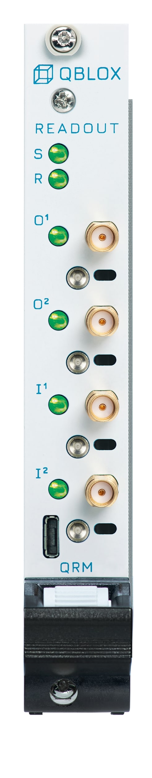
On the front of a QRM module you will find the following components:
4 x SMA female (receptacle) connectors: 2 outputs (O[1-2]: 1 Vpp @ 50 Ω) ; and 2 input channels (I[1-2]: 2 Vpp @ 50 Ω).
4 x SMP male (pin) connectors: Marker output channels (0-3.3 V TTL).
6 x status LEDs: See section Frontpanel LEDs for details.
These input paths use two processing paths (from here on also referred to as path 0 and 1). The module has 6 readout sequencers on board with the following architecture:

Each sequencer in the QRM is connected to all 4 markers and each sequencer can access the outputs and inputs of the QRM. Each readout sequencer in the QRM has one AWG and one acquisition path.
Using parametrization, each sequencer can target one qubit for readout, allowing multiplexed readout of multiple qubits on the same channel. The AWG can generate the readout pulses and the acquisition paths can process the returned readout data. The acquisition path supports three acquisition modes:
Scope: Returns the raw input data.
Integration: Returns the result after integrating the input data; optionally based on an integration function stored in memory.
Thresholded: Returns the binary qubit value after thresholding the integrated value.
TTL trigger: Returns trigger event counts.
The results of the acquisitions are returned to the user through the qblox_instruments driver.
For a list of available features please go to Features
Block Diagram#

Features#
1. 10 MHz Reference#
Alongside all modules available, the QRM baseband module operates with respect to a 10 MHz reference provided by the cluster.
2. Trigger#
The trigger of the QRM is connected to the cluster and allows for fast synchronization between modules.
3. SYNQ#
The Qblox SYNQ technology enables simple and quick synchronization over multiple instruments, allowing for modules to be started synchronously \( \ll 1\) ns. See section synchronization for more information.
4. LINQ#
The Qblox LINQ technology allows for the results of measurements to be shared between devices, distributing outcomes in < 400 ns.
5. Q1 Sequencers#
The Q1 sequencers are the heart(s) of the QRM instrument. They orchestrate the experiment using a custom low-latency sequence processor specifically designed for quantum experiments. Each QRM has 6 readout sequencers to target multiple qubits with one instrument.
Each readout sequencer has a dedicated AWG path and an acquisition path, which enables parametrized pulse generation and readout.
6. Marker output channels#
Each sequencer has control over the four marker output channels, with the control of each sequencer being OR’ed to
create the final marker outputs. The markers can be dynamically controlled with the set_mrk instruction of the
sequence processor (see section on latched instructions),
but can also, be overwritten with the static marker overwrite parameters ReadoutSequencer.marker_ovr_en() and
ReadoutSequencer.marker_ovr_value(). The marker output range is 0-3.3 V TTL. In RF modules set_mrk is also used
to toggle the switches before the outputs/inputs to enable the respective output/input.
6.1 Setting Markers as Active HIGH/LOW#
The default state of marker is active high (OFF = 0 V, ON = 3.3 V). Users have the ability to change the marker output
from active HIGH to active LOW ( OFF = 3.3 V, ON = 0 V). It can be done using the parameter QRM.marker0_inv_en().
This inversion of marker default states is possible for all marker channels.
7. Sequencer Multiplexer#
Each of the 6 readout sequencers in a QRM has two output streams (path 0 and path 1 also called I and Q). Each of these can be connected to any of the two output DACs using the channel map. Similarly, each of the ADCs may be connected to the input streams of any sequencer.
ReadoutSequencer.connect_out0()connects a sequencer path to an output. For example, to connect the Q path of sequencer 2 to output 1, useqrm.sequencer2.connect_out1("Q"). The argument may be “I”, “Q” or “off”. All the output streams that are connected to the channel map are added together. This may result in clipping.ReadoutSequencer.connect_acq_I()connects an input to a sequencer path. For example, to connect input 1 to the I path of sequencer 2, useqrm.sequencer2.connect_acq_I("in1"). The argument may be “in0”, “in1” or “off”. All the sequencers whose input streams are connected to an input receive the same input samples.
For more details about multiplexing and its operation on our cluster, please refer to the multiplexed sequencing tutorial.
Note
The default state is that the I quadrature is connected to all even inputs and outputs of all sequencers, and Q to odd inputs and outputs. This is so that the modules can always play a sequence in their default state.
The channel map may be cleared by setting all connect_out* and connect_acq_* parameters for all sequencers to ‘off’.
The QRM.disconnect_outputs() and QRM.disconnect_inputs() convenience functions may be used instead.
The QRM supports both an IQ (both paths are modulated for use with an IQ mixer) and a real sequencer mode (only path 0 is modulated, and both paths will be combined at the output). See the user guide page for more details.
8. Digital Offset#
Each output has a dedicated offset step statically configured using the QRM.out0_offset(), QRM.out1_offset()
parameters corresponding to each output channel. This is a digital offset applied on top of the combined signal from all
sequencer paths mapped to the corresponding output channel.
9. DAC#
The maximum output and input range of the QRM is 1 Vpp and it is 50 Ω terminated.
10. ADC#
The maximum input range of the QRM’s ADCs is 2 Vpp and 50 Ω terminated.
Note
The 12-bit ADCs have a fixed range of 2 Vpp. When performing acquisitions the input should be an order of magnitude such that the resolution (0.5mV) of the ADC can accurately define the measured signal. Gain or attenuation stages may be required at the input to compensate for this.
11. Input gain#
Dedicated amplifiers provide additional gain to the input signals. A variable gain between -6 dB and 26 dB can be set
using the QRM.in0_gain() parameters. Note that there is also an additional, fixed amplification of 6 dB on on each
input path separate to the variable amplifiers mentioned in previous sentence.
Absolute Maximum Ratings#
Warning
This section shows the absolute maximum ratings of the cluster QRM module. Operation beyond these values can damage the module and cluster!
Parameter |
Condition |
Min |
Typ |
Max |
|---|---|---|---|---|
Voltage applied to output |
-5V |
+5V |
||
Voltage applied to input |
-2.5V |
+2.5V |
||
Marker load impedance |
66Ω |
Specifications#
Output#
Parameter |
Condition |
Min |
Typ |
Max |
|---|---|---|---|---|
Number of channels |
2 |
|||
Output coupling |
DC |
|||
Resolution |
12bits |
|||
Output impedance |
50Ω |
|||
Output range |
In 50Ω load |
+-0.5V |
||
Power Consumption |
32W |
Input#
Parameter |
Condition |
Min |
Typ |
Max |
|---|---|---|---|---|
Number of channels |
2 |
|||
Input coupling |
DC |
|||
Resolution |
12bits |
|||
Input impedance |
50Ω |
|||
Input range |
settable amplification |
+-0.025V |
+-1V |
Marker Outputs#
Parameter |
Condition |
Min |
Typ |
Max |
|---|---|---|---|---|
Number of markers |
4 |
|||
High voltage |
in high Z load |
3.3V |
||
Low voltage |
0.0V |
Typical Performance#
Output#
Parameter |
Value |
Test specifics |
|---|---|---|
Voltage range |
+-0.5 V |
Measured with a 1MHz block wave in 50Ω load |
Rise/Fall time |
<1.3 ns |
Measured with a 1V step in 50Ω load, 10% - 90% |
Settling time |
<8 ns |
Measured with a 1V step in 50Ω load, settled within +-1% |
Overshoot |
<1% |
Measured with a 1V step in 50Ω load |
Crosstalk step |
<-75 dB |
Measured with a 1V step in 50Ω load |
Crosstalk sine |
<-70 dB |
Measured with a 100MHz 1Vpp sine wave in 50Ω load |
Frequency response |
>300 MHz |
Bandwidth (-4dB) |
Frequency response |
>400 MHz |
Bandwidth (-7dB) |
Wideband noise |
<5 nV/sqrtHz |
Noise measured at 121Mhz with 1kHz band and 0V output |
Output RMS noise |
<70 uVrms |
Based on bandwidth and wideband noise |
Signal to noise ratio |
>87 dB |
Based on the output RSM voltage O8 |
Total harmonic distortion |
THD <0.0012 |
Measured at 100MHz sine wave up to the fifth harmonic |
HD2 |
HD2 <-59 dBc |
Measured at 100MHz sine wave up to the fifth harmonic |
HD3 |
HD3 <-60 dBc |
Measured at 100MHz sine wave up to the fifth harmonic |
Input#
Parameter |
Value |
Test specifics |
|---|---|---|
Voltage range |
+-1 V |
|
Rise/Fall time |
1.5 ns |
10% to 90% |
Overshoot rise |
1.8% |
|
Overshoot fall |
4% |
|
Settling time |
30 ns |
Settled within +-1% |
Input-input crosstalk |
<-90 dB |
|
Frequency response |
>350 MHz |
Bandwidth (-3dB) |
Frequency response |
>450 MHz |
Bandwidth (-5dB) |
Low frequency noise at -6 dB gain |
500 uVpp |
0.1-10 Hz integrated |
Low frequency noise at 26 dB gain |
<20 uVpp |
0.1-10 Hz integrated |
Harmonic distortion HD2 |
<= -63 dBc |
~1 dBm input |
Harmonic distortion HD3 |
<= -65 dBc |
~1 dBm input |
SNR -6 dB gain |
~60 dB |
|
SNR 26 dB gain |
~50 dB |
|
Wideband noise at -6 dB gain |
< 43 nV/sqrtHz |
At 100 MHz |
Wideband noise at 26 dB gain |
< 4 nV/sqrtHz |
At 100 MHz |
Wideband noise at -6 dB gain |
<700 uVrms |
integrated over 300 MHz |
Wideband noise at 26 dB gain |
<60 uVrms |
integrated over 300 MHz |
Product Compliance Information#
Compliance with EMC requirements is only guaranteed with cables up to 30 meters.